Abstract A team from the Center for Nano Engineering Research (CRNE) and researchers at the Department of Electrical Engineering, University of Barcelona, have introduced a more efficient and cost-effective method for producing crystalline silicon. Their findings were recently published in the Journal of Applied Physics. This new technique enables the creation of extremely thin silicon wafers—just 10 microns thick—which hold great promise for microelectronics, especially with the growing demand for 3D integrated circuits. The innovation also opens up new possibilities for photovoltaic technology, particularly in the development of flexible solar batteries.
In recent years, there has been a significant push toward thinner silicon wafers. The thinnest achievable through traditional wire-cutting methods is around 150 microns, but this process is inefficient, as nearly half of the material is lost during cutting. The new approach developed by the research group offers a one-step solution that not only improves efficiency but also reduces costs significantly.
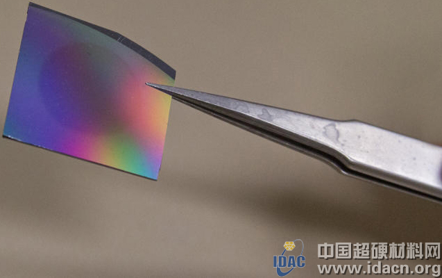
The method involves creating tiny pores on the surface of the silicon material under high-temperature conditions. These pores are precisely controlled to determine the final thickness and number of wafers produced. Once formed, the wafer can be easily separated using a blade-like tool, allowing for accurate control over both the size and thickness of each individual wafer. For instance, a single 300 mm-thick wafer can be split into up to 10 thinner slices, each measuring between 5 and 7 mm in thickness.
Reducing Costs in Industrial Production
The demand for ultra-thin silicon wafers is rising rapidly across industries such as MEMS and photovoltaics. However, conventional cutting techniques have reached a plateau, with current wafer thicknesses hovering around 180 microns. While efficiency has improved and costs have dropped, further reduction in thickness has become increasingly challenging. This new method addresses that challenge effectively, enabling production of wafers as thin as a few tens of micrometers while maintaining strong light absorption and photoelectric conversion capabilities. This breakthrough could lead to more affordable and sustainable energy solutions in the future.
Inoculating Loops &Cell Spreader &Cell Scraper
Bactrial Cell Spreader,plastic spreader microbiology,spreader for microbiology,Corning Platic Cell Lifter
Taizhou TOPAID Medical Device Co,,ltd , https://www.topaidgen.com