Abstract A team from the Center for Nano Engineering Research (CRNE) and the Department of Electrical Engineering at the University of Barcelona has introduced a groundbreaking, more cost-effective, and efficient method for producing crystalline silicon. Their findings were recently published in the latest edition of the *Journal of Applied Physics*. This innovative technique allows for the creation of extremely thin silicon wafers—just around 10 microns thick—which are highly sought after in microelectronics, particularly with the rapid development of three-dimensional integrated circuits. The advancement in silicon technology also opens new possibilities for photovoltaic applications, especially in the field of flexible energy storage systems.
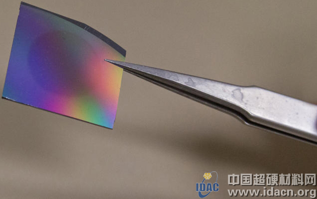
The demand for ultra-thin silicon wafers is growing rapidly, especially in the MEMS industry and solar energy sector. Traditional cutting methods have reached a point where further reductions in thickness are becoming increasingly difficult, despite improvements in efficiency and cost reduction over the past few decades. The new method developed by the research group addresses this challenge effectively. Even at a thickness of just a few tens of micrometers, the wafers maintain their ability to absorb sunlight and convert it into electricity, making them highly suitable for next-generation photovoltaic technologies. This innovation could significantly impact the future of semiconductor manufacturing and renewable energy systems.
Mechanical Micro Pipette,Serological Filler Controller,Micro Pipettor Holder,Micro Pipette Rack Holder
Taizhou TOPAID Medical Device Co,,ltd , https://www.topaidgen.com