I have seen a kind of stereo book with a small house or castle standing up. Inspired by this children's toy book, researchers in China, the United States, and South Korea have developed a particularly simple "pop-up" three-dimensional molding technique that can prepare micro-nano semiconductor devices that cannot be realized by existing 3D printing technologies. This achievement was published in a new issue of the American Journal of Science. Zhang Yihui, an assistant professor of research at Northwestern University, one of the research leaders, told Xinhua News Agency reporters that this technology is called "flexion-guided three-dimensional molding technology." Compared with the existing 3D printing technology, it has many advantages, "it can not be completely Replace existing 3D printing technology, but it can be used as a very important supplement."
"Pop-up" technology for micro-nano semiconductor devices
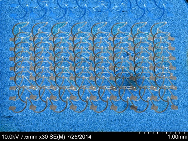
The basic steps of this technique are: first to form a planar structure with a certain configuration, transfer it to a stretched elastic substrate, and selectively bond the planar structure to the elastic substrate by surface chemical treatment, and then release The pre-stretching of the elastic substrate allows the planar structure not adhered to the substrate to be ejected to form a three-dimensional structure.
Zhang Yihui said that one of the advantages of this technology is rapid prototyping; the second is applicable to all types of materials, including semiconductors, metals, polymers, etc.; and the third is compatible with the two-dimensional manufacturing technology of the modern semiconductor industry and can be very complex to form. Three-dimensional structure, they have realized more than 40 kinds of three-dimensional structure, including peacocks, flowers, tables, baskets, tents and starfish, etc.; four is no obvious size limit, the minimum thickness has been achieved is about 100 nm, the maximum thickness of about 1 Mm. The main disadvantage of this technique is that the three-dimensional structure that can be formed still has certain limitations and does not form all the given three-dimensional structures.
Diamond Sharpening Stones is a Abrasive Honing Stones have man made diamonds bonded to a hard, rustles surface which provides an abrasive surface that is harder than any other material - Diamond Stones are very sharp and capable of lasting almost indefinitely. Use Diamond Stones to sharpen or lap almost anything, from tool steel to carbides to glass and ceramics (including ceramic stones). Whenever practical, wetting the stones with water or light oil will virtually eliminate clogging while you sharpen,but they can be used dry as well.
One of the most common arguments for using diamond sharpening plates is that they are flat and do not become hollowed out during their working lives. The first point is only partly true, as the flatness of the plates depends a great deal on the quality of, and the method used to manufacture the plate. But it is true that they do not become hollow in use, like other kinds of sharpening stones do.
Special Diamond Tool,Diamond Sharpening Stone,Rotary Diamond Bit,Polishing Honings Stone,Abrasive Honing Stones
Hans Superabrasive Material Co., Ltd. , http://www.hansuperabrasive.com