Progress in the study of gallium nitride interface states in microelectronics
Recently, Liu Xinyu’s team, a researcher at the High Frequency and High Voltage Center of the Institute of Microelectronics of the Chinese Academy of Sciences, has made progress in the field of GaN interface state research. The LPCVD-SiNx/GaN interface has achieved atomic level flat interface and international advanced interface state characteristics, and proposed suitable The U-shaped distribution function of the interface state with a wider energy range realizes the separation of the discrete energy level and the interface state.
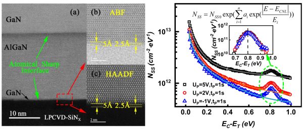
Enhanced GaN MIS-HEMT is a technical route that has not yet been successfully commercialized. The problem of the interface state between GaN and the dielectric is one of the main factors restricting the reliability of the device. Preliminary studies have found that LPCVD-SiNx has the advantages of high temperature tolerance, high film quality, compact structure, no ion damage, and high TDDB characteristics. It is expected to be used as a highly reliable MIS-HEMT gate dielectric and passivation material. However, the high growth temperature of traditional LPCVD-SiNx may cause thermal decomposition and thermal reaction on the surface of the material, especially the etched surface. At the same time, high-temperature processes (for example, ohmic alloys above 800°C) will cause the hydrogen bonds of the passivation site to be destroyed, causing a certain degree of degradation of the dielectric interface, causing random changes in bond length and bond angles in disordered rough crystallization regions and gradient changes The amorphous region is generated, causing uncontrollable frequency dispersion and hysteresis in the device. To avoid the above disadvantages, the prepared robust interface needs to have atomic level flatness and long-range ordered crystal regions with minimal degeneration.
On the other hand, due to the wide distribution of defect electron capture cross-sections in wide band gap semiconductors, both ultra-shallow and deep-level interface states may affect the frequency dispersion and current collapse of the device. Therefore, it becomes very meaningful to evaluate the interface state in a wider energy range. The constant-capacitance deep-level transient Fourier spectroscopy technology can realize the test in the temperature range of 10~400K, which provides an effective characterization solution for the above requirements. However, the detection density of interface state and discrete level defects in multilayer materials is usually coupled, which makes the defect analysis of the dielectric/III-N interface more complicated. It is necessary to use the interface state distribution function to separate the interface state and discrete defect level. Although the U-shaped model based on the DIGS theory is suitable for the interface state distribution of continuous energy levels, it still has some limitations on a wider energy range.
The research work proved that the low thermal budget process is one of the effective means to achieve high-quality interface, including: LPCVD-SiNx growth temperature is reduced from 780℃ to 650℃, and the ohmic alloy temperature is reduced from 850℃ to 780℃. The difficulty lies in reducing the temperature window and ensuring high-quality films and ohmic contacts. Finally, a 2.5-5 angstrom atomic level flat interface is realized between LPCVD-SiNx and GaN. The interface state density is about 1.5×1013 cm-2eV-1 at ET=30 meV, and about 4×10¹¹~1.2 at ET=1 eV. ×1012 cm-2eV-1 level. The team innovatively proposed a physical parameter-based U-shaped distribution function of interface states that is suitable for a wide energy range, and realized the effective separation of discrete energy levels and interface states in multilayer materials. The result was published on Applied Surface Science under the title Suppression and characterization of interface states at low-pressure-chemical-vapor-deposited SiNx/III-nitride heterostructures.
This work was funded by the National Natural Science Foundation of China's major instrument projects, key projects, general projects, and frontier key projects of the Chinese Academy of Sciences.
Atomic level flat interface, advanced level interface state density and U-shaped distribution function
CA Temporary Fence Introduction:
Temporary Fence is also called
Construction Fence,Removable Fence and Portable Fence. This type was
very popular in Canada, the United States, and some other America
countries.
It is quick to be set up and easy to move and is ideal for restricting
access or containing a site and is commonly seen at construction sites,
public events, as a dog run, or anywhere crowd control is important.
It offers the benefits of affordability and flexibility.
Ca Temporary Fence,Temporary Fencing Panel,Construction Temporary Fence,Temporary Construction Fence Panel
HeBei Bosen Metal Products Co.,Ltd , https://www.hbbosenfence.com